INTRODUCTION
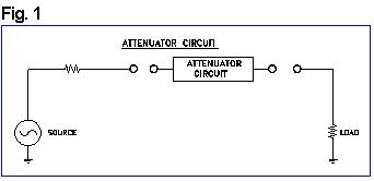
Attenuators are transmission line components with at least two ports used to reduce the input power in a system by a predetermined amount. A switch is generally used in only two states "on" or "off". In contrast the variable attenuator is operated throughout its entire dynamic range. Consider the following circuit (Fig. 1):
The attenuation, %, of a circuit inserted in a transmission line is defined at the ratio in decibels of power incident to the diode, Pi, to power transmitted past the circuit to the load, Pt.Therefore % = 10 log There are two major categories of attenuators: Fixed and variable. Fixed attenuators are those whose attenuation is factory preset at some nominal level. It is a fixed value and cannot be changed. Variable attenuators, on the other hand, can be controlled by the user to vary the attenuation level of the device. This can be done by a number of different methods.
Mechanically variable attenuators are normally adjusted through the use of a tuning screw or knob adjustment. Electronically variable attenuators respond to the application of either current (current-controlled) or voltage (voltage-controlled) to the device. Mechanically variable attenuators, due to the necessity of mechanical adjustment are generally not suited to system requirements. Electronic attenuators are more applicable to these applications and are used in many systems, test and lab situations. The balance of this note is concerned with electronically variable attenuators, their characteristics and how to specify them.
PIN DIODE
The control element used in most electronically variable attenuators is the PIN Diode. PIN Diodes are used primarily for control of microwave power from the low MHz frequencies up to millimeter waves. Some typical applications of PIN Diodes are switches, attenuators, limiters, etc. In order to understand the PIN Diode attenuators it is essential to investigate the PIN Diode itself.
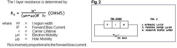
The PIN Diode is a semiconductor device comprised of three layers: The high resistance intrinsic layer surrounded by positive and negatively doped low resistance layers. (See Fig. 2):
Forward bias current carries charges from the conductive layers into the intrinsic layer.
PIN DIODE MODEL
PIN Diodes derive their switching and attenuation characteristics from this variation of the I layer resistance. At zero or reverse bias, RJ is high and the diode acts as a fairly  high-Q capacitor at microwave frequencies. (See Fig. 3) In the forward bias state the I layer resistance is lowered.
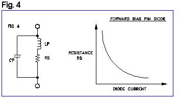
In Figure 4, we can see how the PIN Diode acts as a current controlled RF resistor. An increase in bias current will result in a decrease in RF resistance. It is this factor which makes the PIN Diode so useful in attenuator circuits.
SIMPLE DIODE ATTENUATORS
One of the simplest forms of variable attenuators is the simple shunt diode type seen below. (Fig. 5)

With this type of attenuator the user will supply bias current to the PIN Diode. As current increases the PIN Diode resistance will decrease and the attenuation will increase. At zero or reserve bias the diode will be in its "off" state and the attenuator will be in its low loss state.
MULTIPLE SHUNT DIODE ATTENUATOR
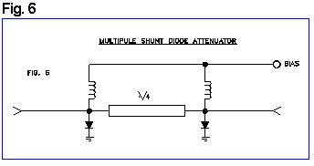
A single shunt element attenuator has obvious limitations. For example, a diode of 1.0 ohm resistance will give about 28 dB of attenuation. It is clear that some other means must be used to achieve higher attenuation.
When a second shunt element is placed 90 degrees (electric spacing), (see Figure 6), from the first the maximum attenuation achievable can be dramatically improved. For example, two diodes each capable of 28 dB attenuation spaced 90 degrees apart will give an attenuation level of 62 dB.
This technique can be extended to three or more elements and is extensively used in PIN Diode attenuator design.
LIMITATION OF SIMPLE ATTENUATORS
Though these simple circuits can operate usefully as attenuators they share common performance limitations: they are reflective in the attenuation range. As attenuation is increased, the VSWR will degrade. For example, a three shunt diode attenuator biased for 40 dB of attenuation will have a VSWR of about 6.0:1. Reflected power can occasionally be a serious problem for a systems designer. Where high VSWR during attenuation levels is a problem, an absorptive attenuator design is a better choice for the system designer.
ABSORPTIVE ATTENUATORS
The absorptive attenuator offers the system designer low VSWR through its entire dynamic range. Examples of absorptive attenuator circuits include switched-bit, Hybrid coupled, and T Pad (both shunt transformed and classical).
SWITCHED-BIT ATTENUATOR
This circuit differs from the other circuits discussed for far that a resistive ‘J’ or B’ attenuation circuit is switched in and out of the network. (See Fig. 7)
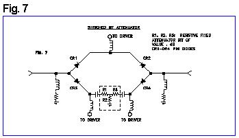
For low loss (insertion loss) state, CR1 and CR2 are biased "on" (low-loss state); CR3 and CR4 are biased "off". When attenuation is programmed, CR1 and CR2 are shut off; CR3 and CR4 are biased on. This introduces an attenuation bit comprised of R1-R3 into the through-line path yielding % dB of attenuation. Essentially the attenuator bit is switched in and out of the circuit, thus giving the name "Switched-bit".
In this note, Switched-bit attenuators differ from other electronic attenuators in the fact that the attenuation elements are fixed resistive T-Pad bits not Pin Diodes.
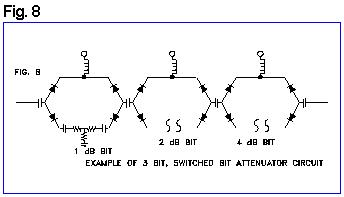
Many sections like that above can be cascaded to give higher levels of attenuation. (See Fig. 8) The lowest value attenuation bit is referred to as the least significant bit and the highest value as the most significant bit.
Switched bit attenuators offer a number of features to the system designer. Distortion generated by the attenuator is low since the power is absorbed in resistive elements and not in the PIN Diodes. The switched-bit attenuator is very temperature-stable because the PIN Diodes are not used over the entire dynamic resistance range, they are simply used as switch elements, switching the attenuation bits in and out of the circuits.
One major drawback with this circuit is that it will have a high insertion loss. As shown in figure 8, there are two series elements per attenuation bit. The more series elements involved the higher the resulting insertion loss. For example, a 6 bit attenuator with a 3 ohm PIN Diode would have 36 ohms of resistance exclusive of other circuit losses. Also, when the least significant bit is 0.5 dB or less, monotonicity is difficult to achieve due to differences in coil resonances, diode loss and other considerations between the insertion loss path and the attenuation path. The switched-bit attenuator is limited in its resolution, being limited by the value of the least significant bit.
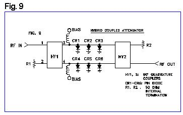
HYBRID COUPLED ATTENUATOR
The attenuator offers good VSWR at any level of attenuation, and its operation is fairly simple. (See Fig. 8)
RF power is incident to HY1. Power is split between the two transmissions paths (one comprised of CR1-CR3, and the other through CR4-CR6). As forward bias is sent to the diodes they conduct and reflect back power to port 3 and 4. Due to the design of this coupler the power from ports 3 and 4 are combined to port 2 and absorbed in the internal termination R1. This results in very low reflected power at port 1.
PMI’s series of attenuators use this circuit topology. The use of low-loss lange couplers manufactured to ±.0001" tolerance Silica substrates ensure superior performance.
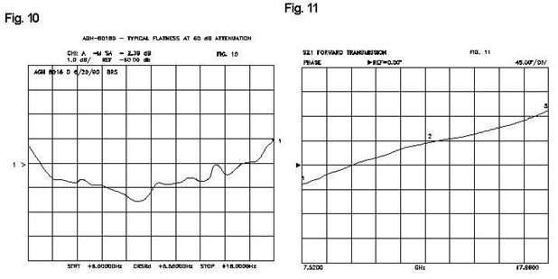
This kind of attenuator has a practical bandwidth limitation of 3.0:1. Application of this technique in a well designed attenuator circuit will yield excellent and repeatable performance. For example PMI is manufacturing sizeable quantities of these attenuators in the 6–18 GHz bandwidth with typical insertion losses of under 3.0 dB and return loss of greater than 11dB across the full bandwidth. The PMI series of attenuators also offer good frequency flatness (3dB P-P at 60 dB) with well-behaved Phase shift characteristics. (See Figs. 10 and 11).
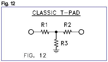
T-PAD ATTENUATOR
The circuit of Fig. 12 is comprised of three microwave resistors. For each value of attenuation there is an ideal value for R1, R2, R3 which (a) gives the correct level of attenuation and (b) maintains a 50 ohm impedance thus insuring a low VSWR. This circuit can be synthesized using PIN Diodes as the variable RF resistor (See Fig. 13). CR1 and CR2 are the series equivalent of R1 and R2.
Direct synthesis of the T-Pad circuit can be difficult and costly to achieve. A much simpler approach is to mount all three PIN Diodes in shunt, making the outside diodes (CR1, CR2) the shunt transformed equivalent of R1, R2 in Fig. 12. This circuit is the so-called folded T-Pad or shunt transformed T-Pad circuit shown in Fig. 13. The shunt impedances are the transformed equivalents of the circuit elements of the classical T-Pad.
CR1 and CR2 are biased independently from CR3. By proper selection of bias current the folded T-Pad design can yield reflection less attenuator performance.

This circuit is very easy to manufacture. PMI has been manufacturing this type of attenuator for many years. It is in-expensive and offers reasonable performance for octave bandwidth requirements. However, this type of circuit has a number of limitations. The circuit is limited to an octave bandwidth. Beyond an octave the frequency flatness and VSWR become degraded. Also the unit-to-unit uniformity of this attenuator is not as good as other types of circuits. The maximum attenuation achievable is limited (usually to under 30 dB), and its frequency flatness is poor compared to a hybrid coupled attenuator.
"TEE PAD"
For applications requiring greater bandwidth PMI is manufacturing PIN Diode attenuators which are essentially variable T-Pads. (See Fig. 15)
 CR1 and CR2 are equivalent to R1, R2, CR3, to R3. The PIN Diodes are varied by changing bias current. Series bias current is used to adjust CR1, CR2 until they reach the value of the series elements in the classical T-Pad of Fig. 12. Likewise CR3 is varied via shunt bias current. By properly selecting series and shunt currents, the attenuator can be varied and the match will be maintained as the resistance of the PIN Diodes will be equivalent to the values of the classical T-Pad. As attenuation is increased, the current through CR3 will increase and the current through CR1 and CR2 will decrease. Two sections of the above circuit are cascaded to achieve the 60 dB level.
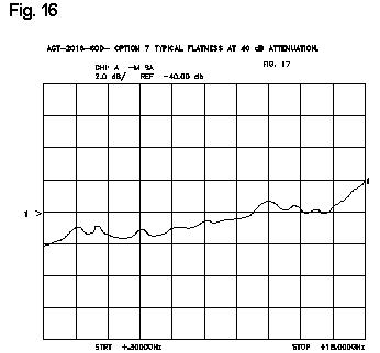
This attenuator, if properly designed, will give the widest bandwidth coverage of all the attenuator types discussed in this application note. Figure 16 shows typical performance on production units.
DRIVER CONSIDERATIONS CURRENT CONTROLLED
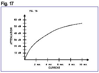
This group of attenuators is driven by current supplied by the user. Some attenuator circuits are commonly sold as current controlled devices. For example, AGH series hybrid coupled devices are often driven directly from current sources. A typical attenuation vs. Current curve can be seen in Figure 17.
Though this is the simplest drive requirement, it does have certain limitations. The current vs. Attenuation curve will follow the PIN Diode exponential function of Rs vs. I. This works fine in a closed loop situation (such as a leveling application) however, its lack of linearity argues against its use in an open loop condition.
ANALOG VOLTAGE CONTROLLED DRIVER CONSIDERATIONS
Voltage-controlled attenuators are controlled by the application of control voltage by the user. They fall into two broad categories: linearized and non-linearized.
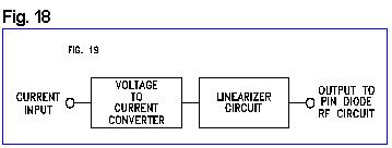
Linearized voltage controlled attenuators are those which follow a specified voltage-to-attenuation transfer function, and non-linearized do not. An example of a linearized attenuator is the American Microwave AGH-D series. This product has an Integral voltage-to-current converter (linearizer) (See fig. 18) which gives the unit a linear voltage to attenuation transfer function. Standard transfer function on this unit is 10 dB/volt, though many different curves can be accommodated.
The linear transfer function is accomplished by using a five break point piece-wise approximation to the diode Rs vs. I curve.
The T-PAD attenuator circuit of FIG. 15 requires two such driver circuits. (One to control the series diodes and one to control the shunts.)
DIGITAL VOLTAGE CONTROLLED DRIVE CONSIDERATIONS
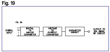 Thus far our discussion has concentrated on analog voltage control drivers. PIN Diodes attenuators can also be controlled by digital methods. For example, the analog control signal used to control the linearized driver circuit of Fig. 19 can be derived from a digital source by means of a Digital-to-Analog Converter. Fig. 19 shows such a driver circuit.
Both AGH-series hybrid coupled and AGT-series T-Pad attenuators are available with an 8 bit digital driver, known respectively as the AGH-DD series and AGT-DD series.
DRIVER CONTROL FOR SWITCHED-BIT-ATTENUATORS
Normally each attenuation bit is driven from an individual control line. Consider the circuit of Figure 8 (3 bit, 1 dB, LSB, 7 dB total attenuation). Assume that a logic ‘I’ is used to enable the bit, the logic table would be as shown below:
DIGITAL WORD | |
MSB 4 dB | 2 dB | LSB 1 dB | Attenuation Achieved |
0 | 0 | 0 | Insertion Loss |
0 | 0 | 1 | 1 dB |
0 | 1 | 0 | 2 dB |
0 | 1 | 1 | 3 dB |
1 | 0 | 0 | 4 dB |
1 | 0 | 1 | 5 dB |
1 | 1 | 0 | 6 dB |
1 | 1 | 1 | 7 dB |
ATTENUATOR TERMS AND DEFINITIONS
Attenuation: General term describing decrease of signal amplitude in transmission from the input to the output of the device the ratio of input to output power. It is commonly expressed in logarithmic terms (dB).
Insertion Loss: the ratio of the power delivered to the load without the attenuator to the power delivered to the load with the attenuator present. In the case of the variable attenuator its insertion loss is measured with the attenuator set to its low loss state.
VSWR: Voltage standing wave ratio (ratio of reflected to incident power) present at the input or output of the attenuator.
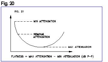
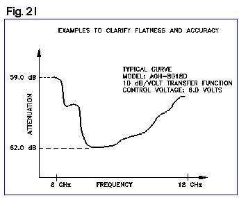
Flatness: Peak to peak variation of attenuation through the specified frequency range. Normally specified in dB. See Fig. 21.

Transfer Function: The relationship between attenuation and control voltage normally specified in dB/volt. This specification is applicable to analog voltage controlled attenuators only.

Accuracy (sometimes called "Linearity"): It is the maximum deviation of the nominal attenuation from the programmed attenuation, normally expressed in dB. This term is used to quantify how accurately the attenuator confirms to the specified transfer function.

Phase Shift (Absolute): The transmission phase angle of the signal at the output of the attenuator relative to the phase angle at the input of the device.
Phase Shift vs. Attenuation: The transmission phase angle of the signal at the output at a given frequency and attenuation relative to the phase angle at the output of the device at the same frequency with the attenuator set to insertion loss. Measured by normalizing absolute phase shift of the unit at insertion loss.
Temperature Coefficient of Attenuation: Measure of how the attenuation changes at a given voltage (current) and frequency as temperature is varied. Normally expressed in dB/E Centigrade. Compensation networks can be designed to minimize the attenuation drift over temperature. For example, a thermistor circuit keeps the typical drift to under .01 dB/EC.
Switching Speed: The time it takes for the attenuator to switch states from one attenuation level to another. Usually referenced from a point on the drive control waveform. Linearized voltage controlled attenuators are generally slow switching from attenuation to insertion loss because the drive circuit presents a high impedance current source to PIN Diodes that are trying to discharge.
Monotonicity: the condition that exists when every increase in control voltage (or current) will always result in an increase in attenuation at all frequencies. Under no conditions will an increase in voltage result in a decrease in attenuation.
Power Handling: The highest incident power level the attenuator can see without performance degradation (max operating power) or without permanent degradation or destruction (max survival power).